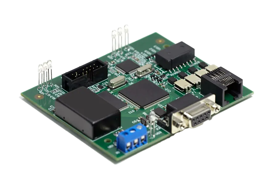
How to Create an Effective Circuit Board Diagram
A circuit board diagram is a logical and visual depiction of a design that can be created using EDA design tools like Altium Designer, Allegro &...

A circuit board diagram is a logical and visual depiction of a design that can be created using EDA design tools like Altium Designer, Allegro &...
Learn the essential steps in the PCB Manufacturing Process from design file conversion to electrical testing and more.
FR4 stands for flame retardant 4 and is commonly used dielectric material in PCB fabrication. It has a Dk value ranging from 3.8 to 4.8
Castellated holes in PCBs establish reliable board-to-board connections.
Whether you're a hobbyist or a professional designer, this blog will guide you through the basics and advanced techniques of soldering.
In this blog, we'll delve into these two surface mount components, exploring their characteristics, applications, and best practices for successful...
This blog will explore the fundamentals of high-speed design and offer essential tips for success in this exciting field
This blog will explore what RoHS is, its significance in PCB manufacturing, and how it benefits both the environment and consumers.
In this comprehensive guide, we will explore the key concepts and considerations for designing successful multilayer stack-ups.
In this blog, we'll provide you with a comprehensive guide on how to create custom footprints in KiCad.
In this blog, we'll delve into the fascinating world of solder mask, exploring its purpose, benefits, application, and importance in design and...
In this blog, we'll explore the various aspects of fab testing and why it's essential for producing reliable electronic devices.
In this guide, we'll walk you through the process of exporting Gerber files from two popular design software tools: Altium Designer and KiCad.
In this comprehensive guide, we will explore what CAM is, its importance, and the key steps involved in this crucial phase of production.
In this blog, we will dive deep into what prepreg is, its types, applications, and how it contributes to the manufacturing process.
This comprehensive guide will walk you through the process of PCB routing in KiCad, from setting up your project to producing a fully routed circuit.
In this guide, we delve into the intricacies of PCBA testing, explore various testing methods, and discuss the role of testing in ensuring the...
In this guide, we'll explore the essential files needed for fabrication and assembly, demystifying the terminology and helping you ensure a smooth...
In this guide, we will explore the process of setting up constraints in Altium Designer, from the basics to more advanced considerations.
In this blog, we'll delve into the art of component placement in KiCad, exploring strategies that can help you optimize your design for efficiency,...
In this blog, we will delve into the key considerations and best practices for designing effective and accurate footprints.
In this blog, we'll dive into what IPC Class 2 PCBs are, their significance, and how they strike the delicate balance between quality and cost.
Follow the step-by-step process of creating a schematic design, from conceptualization to finalizing the schematic in a tool like Altium Designer.
Altium Designer, a leading PCB design software, offers a powerful set of tools for designing and managing vias efficiently.
From choosing suppliers to managing lead times, component procurement can make or break your project's success.
We'll walk you through the process of setting up design rules in KiCad, ensuring that your designs are manufacturable, reliable, and visually...
PCB designs must take into account many factors, like the size and placement of components, the routing of traces, and the use of appropriate...
Altium Designer is a popular software used by engineers and designers to create printed circuit board designs.
Controlled impedance is a critical aspect of PCB design that ensures reliable signal transmission.
Here are some key things you need to know about PCB transmission lines
In this blog post, we will go over the steps required to create a schematic using KiCad.
In this blog post, we'll discuss some best practices for component placement to ensure that the final product functions as intended.
In this blog post, we will explore the different materials used in PCB fabrication and their properties.
In this blog post, we’ll discuss some common DFA errors and provide tips on how to avoid them.
PCB stack-up design is a crucial aspect of the fabrication process. It involves determining the configuration of the layers that make up the board.
Surface mount technology, or SMT, is a method of electronic component placement used in printed circuit board (PCB) assembly.
DFM is the process of ensuring that the design of the circuit board meets certain requirements.